【Articles】The Engineer’s Guide to Pogo Pins: 15 Must-Know Q&As
2026-01-06
The Engineer’s Guide to Pogo Pins: 15 Must-Know Q&As
Pogo Pins (Spring-loaded Probes) serve as a critical interface in semiconductor testing and mass production. Known for their elasticity, thermal stability, and long lifespan, they are vital throughout the IC supply chain. We have compiled the 15 most frequent technical questions regarding their selection, application, and maintenance to help you optimize your testing environment.
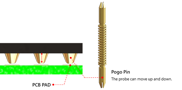
Q1: What are Pogo Pins?
A Pogo Pin is a probe with an internal spring that provides consistent contact force between an IC and a test fixture. It effectively compensates for variations in pad height and pitch, ensuring reliability during high-precision testing.
Q2: What are the primary applications for Pogo Pins?
Pogo Pins are favored for their high durability, stable electrical transmission, and suitability for fine-pitch applications. Key use cases include:
- IC Functional Test
- IC Programming
- PCB / PCBA Testing(ICT / FCT)
- Kelvin Test
- Burn-in Test
- Automated Mass Production Testing
- R&D and Engineering Verification (EVT / DVT)
Q3: What are the advantages of Pogo Pins?
Compared to stamped or clip pins, Pogo Pins offer superior performance:
- Stable Spring Force: Provides consistent axial pressure, maintaining ultra-low contact resistance across hundreds of thousands of cycles.
- Superior Electrical Performance: Due to their precision manufacturing and modular design, Pogo Pins provide shorter and electrically superior signal paths compared to standard stamped or clip pins. This ensures signal stability and integrity during high-frequency testing.
- High Adaptability & Low Maintenance: They feature an exceptionally wide operating temperature range (e.g., -55°C to 175°C), making them ideal for high-temperature Burn-in testing. Furthermore, their individually replaceable design significantly simplifies maintenance workflows and reduces long-term operational costs.
- Exceptional Durability: Specifically engineered to withstand high cycle counts, their long lifespan makes them the ideal choice for high-volume Final Testing (FT).
- High-Precision Contact: The precision manufacturing process minimizes the accumulation of assembly tolerances, which enhances the positioning accuracy of the test points.
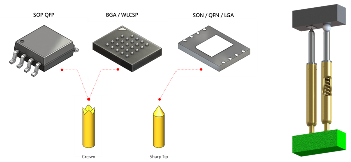
Q4: Which IC package types are suitable for Pogo Pins?
They are suitable for packages such as WLCSP, BGA, QFN, CSP, LGA, and SOP. Selection depends on pad size, pitch, solder ball height, and material. These factors are balanced with the appropriate probe tip shape, travel distance, and spring force.
Q5: What is the lifespan of a Pogo Pin, and how is it defined?
Lifespan is defined as the maximum number of cycles a Pogo Pin can withstand while maintaining reliable test accuracy. A Pogo Pins remains within its functional life as long as it preserves low contact resistance, stable spring force, and its original tip shape. The lifespan ends when tip wear, oxidation, solder accumulation, or force degradation exceeds technical specifications. While most datasheets guarantee a mechanical life of 200K cycles, practical usage typically ranges between 50K and 150K cycles due to real-world environmental factors.
Q6: How do Pogo Pins meet high-speed and high-frequency testing requirements?
High-speed performance is achieved through short-probe designs and impedance matching combined with low-dielectric materials. By maintaining the shortest possible signal path, these Pogo Pins effectively minimize signal reflection and attenuation, ensuring high-frequency integrity.
Q7: Why is contact resistance critical in IC testing?
Contact resistance directly impacts signal accuracy and stability. High resistance can cause voltage drops or signal distortion. Generally, new Pogo Pins must maintain a resistance below 80 mΩ, though high-speed Final Test (FT) requirements may demand even lower values.
Q8: How does spring force affect testing quality?
Excessive force can damage IC pads, while insufficient force leads to poor contact or signal fluctuations. For FT Pogo Pins, the spring force is typically designed between 15g and 35g (±20%).
Q9: What issues can arise if the Pogo Pin travel is too short?
Insufficient travel results in inadequate contact force and unstable contact resistance. This leads to signal attenuation or test failure, which is a particularly sensitive issue for high-speed signals.
Q10: How does the gold plating thickness on FT probe tips affect lifespan?
Plating thickness determines wear resistance and antioxidant capabilities. If the plating is too thin (<1 μm), it can be easily worn through, causing contact resistance to rise. Conversely, excessive thickness can impact tip precision and increase costs. The standard specification for plating thickness is typically 2–3 μm.
Q11: What causes poor contact of Pogo Pins after repeated FT cycles?
Poor contact is typically caused by tip wear, surface contamination, or solder adhesion, all of which reduce the effective contact area and increase resistance. Additionally, spring force degradation can lead to unstable contact with the IC, while fixture alignment errors or variations in solder ball height can further compromise contact reliability over time.
Q12: What are the symptoms of Pogo Pin spring fatigue?
Under high cycle counts, spring fatigue typically manifests as a reduction in rebound force, leading to inconsistent or insufficient contact pressure and elevated contact resistance. In severe cases, the plunger may fail to return to its original position or make full contact with the solder ball. These symptoms can be accurately diagnosed by analyzing spring-force curves and monitoring contact resistance trends during the testing process.
Q13: How to determine when a Pogo Pin needs replacement, and what is the process?
When long-term use leads to rising contact resistance, unstable signals, tip wear, or decreased spring rebound force—and these issues cannot be resolved through cleaning or calibration—replacement is required. Typically, you can directly replace only the individual failed probe. After replacement, a contact resistance and functional test should be performed to ensure the operation has returned to a stable state.
Q14: How do tip debris and residue affect testing?
Dust, oxidation, or flux residue increases contact resistance, leading to signal instability or contact failure. Regular cleaning is essential to maintain performance. We recommend using alcohol with a soft brush for routine maintenance; more aggressive methods, such as nano-steel brushes, should only be used if standard cleaning is ineffective.
Q15: Why choose DediProg Pogo Pins?
Rapid Customization × MIT Quality × IC Industry DNA
- Fast Customization Capabilities: Leveraging our extensive experience in Pogo Pin design and manufacturing, DediProg offers customized tip structures, materials, travel distances, and spring forces tailored to specific IC package types, dimensions, pin counts, and pitch requirements.
- Superior MIT Quality (Made in Taiwan): Our Pogo Pins are designed and manufactured in-house with full process control. From tip structure and spring specifications to final assembly, we maintain consistent standards to ensure contact stability and lifespan while providing a reliable supply at a reasonable cost.
- Proven IC Industry DNA: DediProg Pogo Pins are integrated into our own programming sockets and mass-production solutions. This allows us to continuously optimize tip structures and spring designs based on long-term field feedback. Unlike component-only suppliers, we can rapidly adjust design parameters to meet the IC industry's real-world demands for contact stability and durability.
Read More: Understanding PCR: Applications, Advantages, and Maintenance FAQs
Explore More:
Pogo Pin
Final Test Socket
Open Top Socket
Burn-in Socket
Not sure which testing solution fits your needs? Contact us for a free evaluation.
 |  |  |  |

E-mail: sales@dediprog.com